Use Analog Devices LTC6373 to analyze the case of driving precision ADC
Publish:IC chip, PCB, PCBA, integrated circuit and other electronic components-Shenzhen Hao Qi Core Technology Co., Ltd Time:2022-08-15 Views:215
The market demand for industrial applications is increasing day by day, and data acquisition systems are the key equipment. They are usually used to detect temperature, flow, liquid level, pressure and other physical quantities, and then convert the analog signals corresponding to these physical quantities into high-resolution digital information, which is further processed by software. Such systems are increasingly demanding precision and speed. These data acquisition systems consist of amplifier circuits and analog-to-digital converters (ADCs) whose performance has a decisive impact on the system.
However, the overall accuracy is also affected by the ADC‘s input driver, which buffers and amplifies the input signal. In addition, a bias signal must be added or a fully differential signal generated to cover the ADC‘s input voltage range and meet its common-mode voltage requirements, without altering the original signal in the process. Programmable-gain instrumentation amplifiers (PGIAs) are often used as input drivers. In this paper, we propose a combination of input driver and ADC through which very accurate conversion results can be achieved to build a high-quality data acquisition system.
For example, Analog Devices‘ LTC6373 is a PGIA suitable for high-precision data acquisition systems. In addition to a fully differential output, it features high DC accuracy, low noise, low distortion (see Figure 2), and a high bandwidth of 4 MHz with a gain of 1/4 to 16. ADCs can be driven directly from it, making it suitable for many signal conditioning applications.
The circuit in Figure 1 shows an example of using the LTC6373 to drive a precision ADC, an AD4020 with 20-bit resolution of 1.8 MSPS.
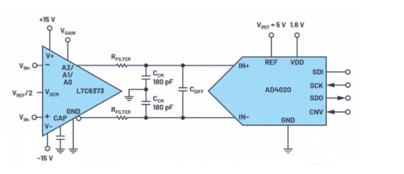
Figure 1. Example of a circuit driving a precision ADC.
In this circuit, the LTC6373 is DC coupled at the input and output, eliminating the need for a transformer to drive the ADC. The gain is programmable from 0.25 V/V to 16 V/V via pins A2/A1/A0. In Figure 1, the LTC6373 is used in a differential input to differential output configuration with ±15 V symmetrical supply voltages. Alternatively, the input can be single-ended, while the output is still differential.
In Figure 1, the output common-mode voltage is set to VREF/2 via the VOCM pin. This enables the output level shifting of the LTC6373. Each output of the LTC6373 varies from 0 V to VREF, so there is a differential signal at the ADC input with a magnitude of 2 × VREF. The RC network between the output of the LTC6373 and the ADC input forms a single-pole low-pass filter that reduces current glitches that occur when switching capacitors at the ADC input. At the same time, the low-pass filter limits the broadband noise.
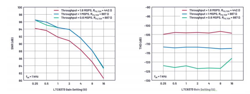
Figure 2. SNR (left) and THD (right) performance of AD4020 driven with LTC6373.
Figure 2 shows the signal-to-noise ratio (SNR) and total harmonic distortion (THD) of the LTC6373 driving the AD4020 SAR ADC (high-impedance mode) over the entire input voltage range (10 V p-p). Satisfactory results can be obtained when the throughput is 1.8 MSPS and the filter resistance (RFILTER) is 442 Ω. The manufacturer recommends an RFILTER of 887Ω at 1 MSPS or 0.6 MSPS.
The LTC6373 can drive most SAR ADCs with differential inputs without the need for additional ADC drivers. However, in some applications, a separate ADC driver can be used between the LTC6373 and the precision ADC to further improve the linearity of the signal chain.
Summarize:
The circuit shown in Figure 1 is optimized for fast, high-precision data acquisition systems. Therefore, the excellent characteristics of the LTC6373 facilitate signal conditioning of the sensor output signal. With the help of the online tool ADI Precision Studio, especially the included ADC driver tool, Analog Devices can provide additional support for this type of amplifier stage, filter and linear circuit design.
Features of the Analog Devices LTC6373:
1. Programmable gain pin: G = 0.25, 0.5, 1, 2, 4, 8, 16 V/V + shutdown;
2. Fully differential output;
3. Gain error: 0.012% (maximum);
4. Gain error drift: 1ppm/°C (max);
5. CMRR: 103 dB (minimum), (G = 16);
6. Input bias current: 25 pA (maximum);
7. Input offset voltage: 92 μV (max), G = 16;
8. Input offset voltage drift: 1.7 μV / °C (max), G = 16;
9. –3 dB bandwidth: 4 MHz, G = 16;
10. Input noise density: 8 nV/√Hz, G = 16;
11. Slew rate: 12 V/μs, G = 16;
12. Adjustable common mode output voltage;
13. Static power supply current: 4.4 mA;
14. Power supply voltage range: ±4.5 V ~ ±18 V;
15. The rated temperature range is –40 °C ~ 125 °C;
16. Small 12-pin 4mm × 4mm DFN (LFCSP) package.
Previous:Renesas Electronics Expands Support for Microsoft Azure RTOS for Its 32-Bit MCU Product Family 2022/09/26
Next:Introduction of Xilinx is Virtex series FPGA products 2022/08/12
Next:Introduction of Xilinx is Virtex series FPGA products 2022/08/12
- CONTACT US
-
-
Contact Person: Mr. Andy Luo
Job Title: Sales
Business Phone: +(86) 13632701337 (electronic component) , +(86)13632701337 (Automation Part )
WHATSAPP: +86 13632701337 (electronic component) , +(86)13632701337 (Automation Part )
Wechat: +86 13632701337 (electronic component) , +(86)13632701337 (Automation Part )
Skype: happylowping
ICQ: 458036258
Email:andyluo@kinglionski.com (electronic component) , andyluo@kinglionski.com (Automation Part )


 happylowping
 Andy
Andy
 'hennry@kinglionski.com '