STM32 chip interpretation
Publish:IC chip, PCB, PCBA, integrated circuit and other electronic components-Shenzhen Hao Qi Core Technology Co., Ltd Time:2022-01-09 Views:711
1. Internal resources of the chip
Kernel:
– 32-bit high performance ARM Cortex-M3 processor
– Clock: up to 72M, can actually exceed the screen a little bit
– Single-cycle multiply and hardware divide
– Single-cycle multiply and hardware divide
Memory capacity:
– STM32F103ZET6: 512K FLASH, 64K SRAM
– STM32F103RCT6: 256K FLASH, 48K SRAM
Clock, reset and power management:
– 2.0~3.6V power supply and IO voltage
– Power-on reset, power-down reset and programmable voltage monitoring
– Powerful clock system
IO port:
–STM32F103ZET6: 144 pins, 112 IOs
–STM32F103RCT6: 64 pins, 51 IOs
– Most IO ports are 5V resistant (except analog channels)
– Support debugging: SWD and JTAG, SWD only needs 2 data lines
Low power consumption:
– Three low power modes of sleep, stop and standby
– Available battery to power RTC and backup registers
AD:
– 3 12-bit AD [up to 21 external measurement channels]
– Conversion range: 0~3.6 (power supply voltage)
– Internal channel can be used for internal temperature measurement
– Built-in reference voltage
DA:
2 12-bit DAs
DMA:
12 DMA channels (7+5=12; 7-channel DMA1, 5-channel DMA2)
Peripherals supported: Timer, ADC, DAC, SDIO, I2S, SPI, I2C, and USART
Timer:
Up to 11 timers
- 4 general purpose timers
- 2 basic timers
- 2 advanced timers
-1 system timer
- 2 watchdog timers
Communication Interface:
Up to 13 communication interfaces
-2 I2C interfaces
-5 serial ports
-3 SPI interfaces
-1 CAN2.0
- 1 USB FS
-1 SDIO
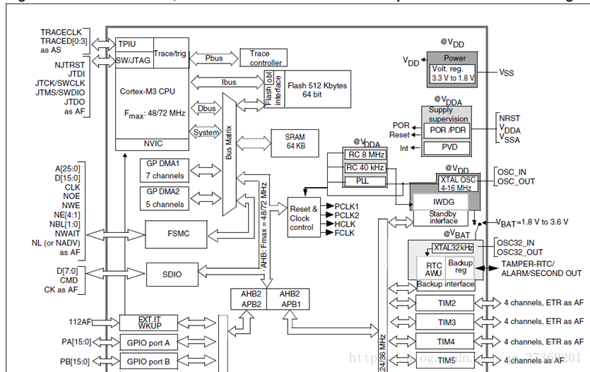
2. the internal structure of the chip


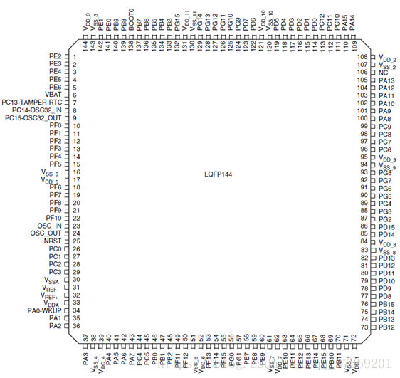
3. Chip pin function diagram

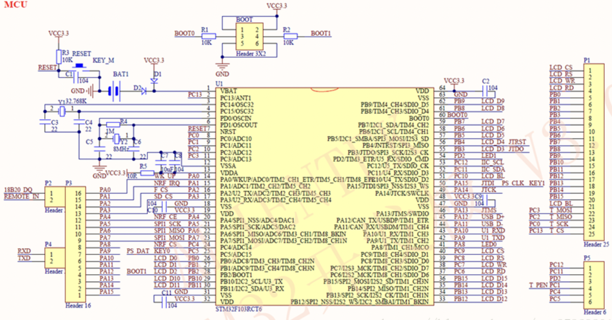
4. STM32 minimum system

powered by
reset
Clock: External crystal oscillator (2)
Boot boot mode selection
Download circuit (serial port/JTAG/SWD)
Backup battery
- CONTACT US
-
-
Contact Person: Mr. Andy Luo
Job Title: Sales
Business Phone: +(86) 13632701337 (electronic component) , +(86)13632701337 (Automation Part )
WHATSAPP: +86 13632701337 (electronic component) , +(86)13632701337 (Automation Part )
Wechat: +86 13632701337 (electronic component) , +(86)13632701337 (Automation Part )
Skype: happylowping
ICQ: 458036258
Email:andyluo@kinglionski.com (electronic component) , andyluo@kinglionski.com (Automation Part )


